DFSX claims an HBM-free AI chip with double NVIDIA's system bandwidth on 14nm
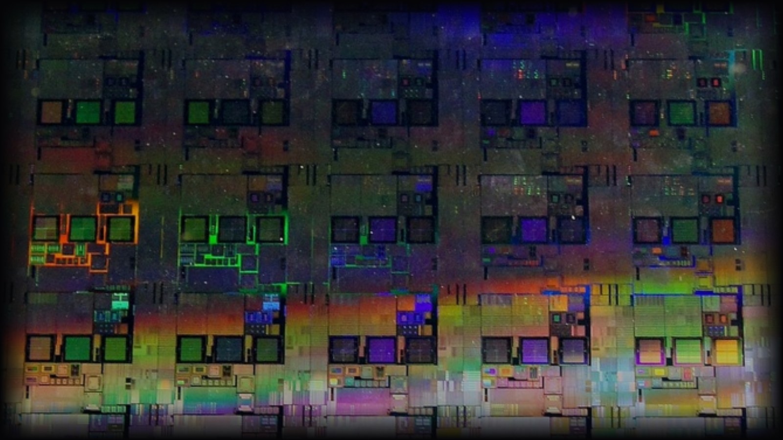
Dongfang Suanxin, known as DFSX, stacks DRAM directly on top of the compute die using 3D wafer-level hybrid bonding. That fuses the copper paths of both layers and removes microbumps entirely. The reason the design exists: it needs no HBM at all, and high bandwidth memory is exactly what export controls have made hardest for Chinese firms to obtain.
The claim
A TY64 SuperNode built from 14nm DF2000 chips delivers 960 TB/s of memory bandwidth, against 576 TB/s for NVIDIA’s GB200 NVL72 system. The already-shipping DF1000 is rated at 6.4 TB/s per chip with 900 GB/s of scale-up bandwidth for chip-to-chip traffic. DF2000 is expected in the fourth quarter of 2026.
Handle with care
Those numbers come from DFSX itself. No independent lab has benchmarked a TY64, and 14nm sits several generations behind the 4nm-class process NVIDIA uses. Bandwidth is also one axis out of many: compute density, yield, power draw and software maturity all decide whether a system is usable at scale.
Why it matters anyway
The strategic idea is the interesting part regardless of whether the specific numbers hold. If you cannot buy the best process node or the best memory, you change where the memory sits. Whether architecture is a real way around export controls, or the process gap wins in the end, is now a live experiment running at national scale.
Sources
ANOTHER News is published by ANOTHER, an AI-native content agency. Daily coverage also runs on Instagram.
Related

Musk's Davos warning that AI will run out of electricity is aging into consensus
Speaking at the World Economic Forum on January 22, 2026, Elon Musk said electrical power is fundamentally the limiting factor for AI deployment, warning that with US generating capacity growing only 3 to 4 percent a year, the industry could soon produce more chips than it can turn on. Months later, data-center power deals and grid bottlenecks dominate the AI infrastructure conversation.
HRL's 18-qubit silicon chip runs its own error detection inside the cryostat
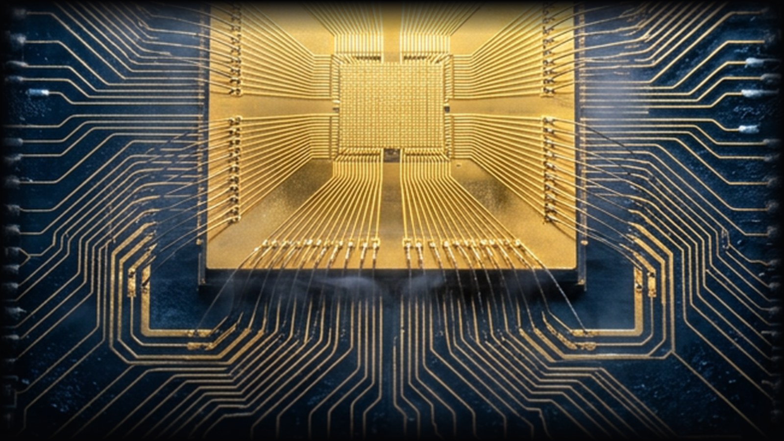
On July 29, 2026, HRL Laboratories published in Nature an 18-qubit silicon spin quantum processor that runs itself, with no racks of room-temperature control electronics. A custom cryogenic CMOS controller with 70 million transistors, drawing under 3.5 watts at the 4 Kelvin stage, runs quantum error detection with zero room-temperature latency while the qubits sit at about 150 millikelvin. Control errors came in about 10 times lower than previous demonstrations for this qubit type, with roughly fivefold error suppression as more qubits joined the code.

ChipAgents raises $60M more to put AI agents inside semiconductor design
On July 29, 2026, ChipAgents extended its Series A to $134 million in total with a $60M round led by B Capital, with Micron, MediaTek and Ericsson among its investors. Its AI agents already run at more than 120 semiconductor companies, annual recurring revenue grew 6x in the first half of 2026, and the startup expanded its Nvidia partnership to build a specialized chip-design model.